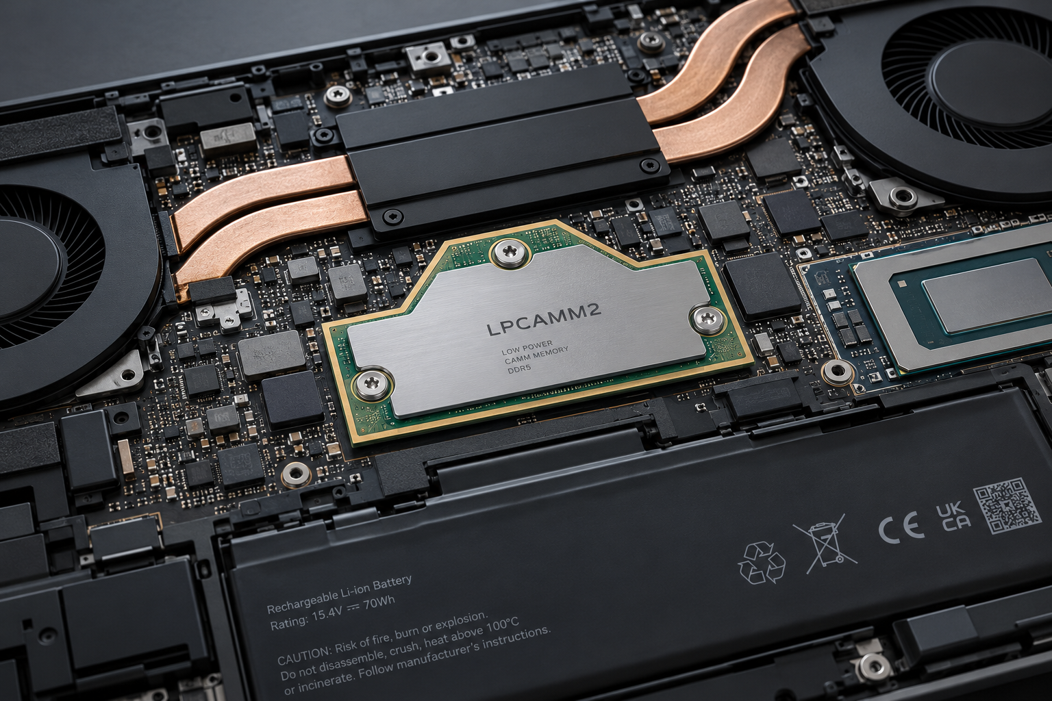
When you unbox a modern ultra-thin laptop, you hold an engineering triumph that is simultaneously an architectural hostage situation. The chassis is carved from a solid slab of anodized aluminum, the display stretches to the perimeter with razor-thin bezels, and the device sips battery power so conservatively that it runs an entire workday on a single charge. Yet the moment you loosen the bottom screws and peer beneath the vapor chamber, you discover a grim reality that has governed portable computing since 2010: the system memory is not a component you can replace, upgrade, or service. It consists of bare silicon dies permanently soldered to the printed circuit board, locked in place by hundreds of microscopic lead-free solder balls under hardened epoxy underfill.
For fifteen years, the personal computer industry insisted this was the non-negotiable cost of progress. If you demanded a lightweight machine with day-long battery life, you were told that dynamic random-access memory had to be soldered directly adjacent to the central processing unit. If you wanted the freedom to expand your memory three years down the road when your workflows grew, your only alternative was to purchase a bulky workstation equipped with Small Outline Dual In-Line Memory Module (SO-DIMM) sockets designed during the late 1990s.
This manufactured compromise created an economic windfall for hardware manufacturers and an environmental tragedy for consumers. Computer makers exploited the absence of modularity by instituting an aggressive tier pricing strategy, routinely charging two hundred to four hundred dollars at checkout for an extra sixteen gigabytes of memory that cost the factory less than thirty dollars to source. Meanwhile, millions of otherwise pristine laptops were prematurely sent to electronic waste recycling facilities simply because a single memory address line developed an intermittent solder fault or because modern artificial intelligence workloads exceeded the fixed capacity chosen on the day of purchase.
That fifteen-year compromise has finally broken down. Under the auspices of the JEDEC Solid State Technology Association, a new open industry standard designated as JESD318 has arrived to dismantle the soldered monopoly. Known commercially as LPCAMM2 (Low-Power Compression-Attached Memory Module), this specification accomplishes what computer engineers spent a decade declaring physically impossible. By replacing traditional friction-fit edge sockets with an ultra-dense, vertical compression Land Grid Array (LGA) connector secured by three standard screws, LPCAMM2 delivers the full speed and power thrift of LPDDR5X memory in a modular, field-replaceable form factor. To appreciate how three small fasteners and a gold-plated compression pad are reshaping portable computing, we must examine why high-speed memory became trapped on the motherboard in the first place.
💻 The Fifteen-Year Curse of the Soldered Motherboard
The story of soldered laptop memory began in earnest in October 2010, when Apple unveiled the redesigned unibody MacBook Air. By eliminating the traditional swappable hard drive in favor of flash memory modules and soldering low-power DRAM directly onto the logic board, computer designers proved that removing modular sockets allowed a laptop to shave millimeters off its thickness and eliminate ounces of structural weight. Within eighteen months, Intel codified this design philosophy into the Ultrabook specification, pushing every major Windows manufacturer from Dell and Lenovo to HP and Asus into adopting soldered memory architectures.
At the time, the transition was justified through the lens of mechanical necessity. Traditional SO-DIMM memory sticks, first standardized by JEDEC in 1997, were chunky rectangular cards measuring roughly sixty-seven millimeters wide and thirty millimeters tall. When inserted into a motherboard, they required a mechanical socket with angled insertion rails, metal retention clips, and substantial vertical clearance. In a dual-channel memory configuration requiring two stacked SO-DIMM slots, the memory subsystem alone consumed more than eight to eleven millimeters of vertical z-height inside the chassis. In a device whose total thickness was intended to be twelve millimeters, dedicating nearly the entire internal height to a plastic memory socket was a mechanical impossibility.
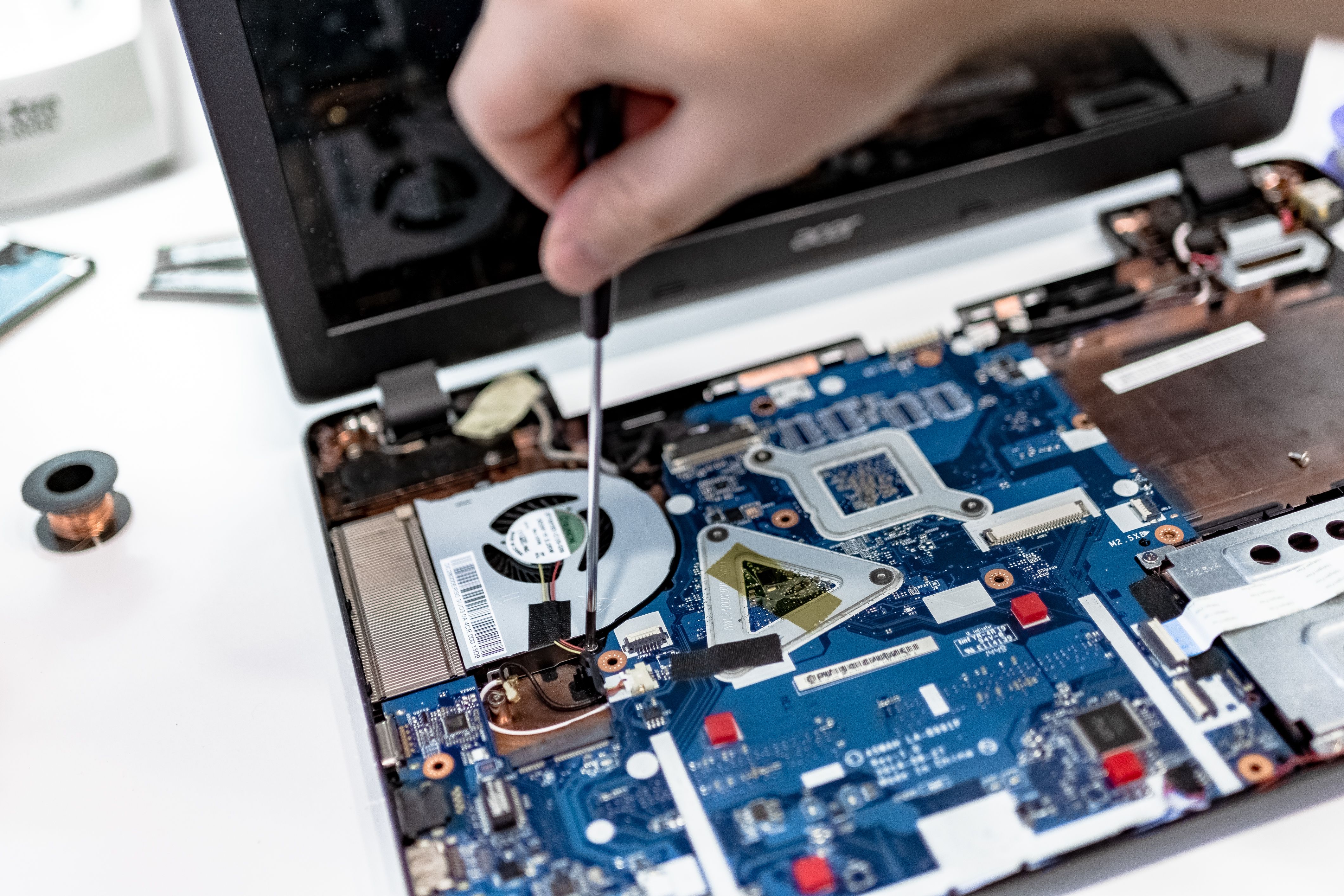
Yet the mechanical bulk of the socket was only the visible half of the problem. A far more significant transformation was occurring on the silicon level. As laptop processors integrated high-performance graphics engines and multi-core architectures, their appetite for memory bandwidth exploded. Standard DDR memory designed for desktop towers consumed substantial idle power because its clock signals and bus termination resistors remained energized even when the processor was displaying a static document. To extend battery life from three hours to ten hours, the industry migrated to Low-Power Double Data Rate (LPDDR) memory.
LPDDR was fundamentally different from standard DDR. It was designed from its inception for mobile phones and tablets, prioritizing low operating voltages, aggressive power-down states, and deeply integrated clock gating. However, LPDDR achieved its power efficiency by demanding extraordinarily tight electrical tolerances. It could not tolerate the electrical parasitics, signal reflections, and impedance discontinuities introduced by legacy mechanical card-edge connectors. As a result, memory manufacturers produced LPDDR exclusively in Ball Grid Array (BGA) surface-mount packages meant to be soldered permanently onto circuit boards.
For more than a decade, this created a rigid market division:
- Workstations and Gaming Laptops: Retained socketed SO-DIMM slots utilizing standard DDR4 or DDR5 memory, offering repairability at the expense of battery life, bulkier profiles, and lower frequencies.
- Ultraportables and Premium Laptops: Adopted soldered LPDDR memory, achieving thin profiles and long battery runtimes at the cost of zero serviceability and locked configurations.
The industry settled into this equilibrium. Consumers were trained to accept that purchasing a laptop meant guessing future memory demands at checkout, paying steep fees for thirty-two gigabytes just in case. If an owner miscalculated, their only recourse was to replace the entire computer. The soldered motherboard had become an accepted fixture of consumer electronics.
📐 Why High-Frequency LPDDR Could Never Use SO-DIMM Sockets
To understand why traditional sockets could not simply be adapted for LPDDR memory, one must venture into the physics of high-frequency transmission lines. On an electrical schematic, a copper trace on a circuit board looks like a simple line that transports current from point A to point B instantaneously. In modern digital computing, where memory buses transfer data at rates exceeding 6,400 to 8,533 megatransfers per second, that copper trace stops behaving like a simple wire and begins behaving like an analog high-frequency radio waveguide.
At frequencies in the gigahertz range, electromagnetic signals travel across a printed circuit board at approximately fifteen centimeters per nanosecond. When a memory controller inside the processor transmits a clock pulse or a data bit across a bus operating at 7,500 megatransfers per second, the duration of each individual data bit on the bus is barely 133 picoseconds. In that minuscule sliver of time, the electrical wavefront travels less than two centimeters along the copper trace. If the physical distance between the processor and the memory chip is too long, or if the signal encounters abrupt changes in electrical impedance along its path, the signal reflects backward toward the transmitter, creating constructive and destructive interference waves that corrupt the data.
Traditional SO-DIMM Signal Path (Signal Degradation):
[CPU/SoC] ===(Long PCB Trace 60-80mm)===> [Socket Solder Leads]
          ===> [Right-Angle Socket Pin] ===> [Card Edge Contact Pad]
          ===> [DIMM PCB Trace 15-25mm] ===> [DRAM Chip]
          * Multiple impedance discontinuities, high capacitive load, capped at 5600 MT/s *

LPCAMM2 Direct Compression Signal Path (Pristine Transmission Line):
[CPU/SoC] ==(Ultra-Short Trace <15mm)==> [Motherboard Land Pads]
          ==[Vertical Compression Interposer]==> [LPCAMM2 Module Pads]
          ==[Sub-5mm Module Trace]==> [LPDDR5X DRAM Chip]
          * Zero right-angle pins, matched 40-ohm impedance, capable of 8533+ MT/s *
A conventional SO-DIMM socket presents an obstacle course to a high-speed digital pulse. First, the memory controller signals must travel from the central processor through dozens of millimeters of serpentine motherboard traces to reach the memory socket. When the signals reach the socket, they transition from the planar circuit board into metal lead pins soldered to the board surface. The signal then travels through the internal curved geometry of the socket pin, crosses the friction-fit pressure contact between the pin and the gold edge fingers of the memory stick, and finally traverses another section of circuit board on the memory module itself before reaching the silicon dies.
Every single one of these physical transitions represents an impedance discontinuity. The junction where a flat trace meets a stamped metal socket pin introduces stray inductance and parasitic capacitance. At modest bus frequencies like DDR3 at 1,600 megatransfers per second, the timing margins were generous enough that the signal could tolerate these small distortions. But as memory standards progressed to DDR5 and LPDDR5X, the timing eye (the tiny operational window in which a receiver can distinguish a logical binary one from a zero) narrowed to a razor-thin slit of picoseconds.
Furthermore, LPDDR memory achieves its energy efficiency by dropping operating voltages to microscopic thresholds. While standard DDR5 operates with a core voltage of 1.1 volts, LPDDR5X operates with an core I/O voltage as low as 0.5 volts and core logic voltage of 1.05 volts. When you cut the signal voltage in half, the electrical signal-to-noise ratio drops proportionally. A voltage drop or ground-bounce ripple that would be completely harmless on a 1.2-volt DDR4 line becomes fatal on a 0.5-volt LPDDR5X bus, triggering unrecoverable bit flips and memory parity errors.
Because standard SO-DIMM slots placed the memory chips forty to eighty millimeters away from the processor and introduced multiple right-angle pin transitions, running low-voltage LPDDR across a SO-DIMM socket was fundamentally impossible. The signals would be completely degraded before they ever completed the round trip. Engineers were left with no choice: to use LPDDR, they had to place the memory chips within ten to twenty millimeters of the processor package and solder them directly to the motherboard with point-to-point traces. The industry gained low power and extreme speed, but it forfeited repairability entirely.
🔩 Inside the JEDEC JESD318 Standard: The Mechanics of Compression
The breakthrough that broke this engineering deadlock did not originate in a memory foundry, but inside the client hardware engineering labs of Dell. In 2020, a small team of engineers led by Senior Distinguished Engineer Tom Schnell began tackling the thermal, spatial, and bandwidth bottlenecks suffocating Dell Precision mobile workstations. Dell recognized that high-performance mobile workstations were hitting a wall: they needed the massive bandwidth and low power of next-generation memory, but their corporate enterprise customers vehemently refused to purchase laptops with non-replaceable, soldered components.
Rather than trying to optimize the 1997-era edge-connector concept, Schnell and his team took inspiration from modern processor sockets. For decades, desktop and server processors from Intel and AMD had avoided pins and edge connectors by utilizing Land Grid Array (LGA) sockets. In an LGA socket, the motherboard features an array of tiny, spring-loaded pins or an elastomeric conductive interposer, while the bottom of the processor chip features an array of flat, gold-plated contact pads. When a retention mechanism clamps the processor down vertically against the socket, hundreds of electrical connections are established simultaneously through pure physical compression, with negligible trace length and uniform impedance.
Dell adapted this compression concept to dynamic memory, engineering a flat, horizontal module known as CAMM (Compression Attached Memory Module). Recognizing that a proprietary standard would remain a niche curiosity, Dell took the step of presenting the technology royalty-free to the JEDEC JC-45 Committee on DRAM Modules. Over three years of cross-industry collaboration involving semiconductor leaders including Micron, Samsung, SK Hynix, Lenovo, and Intel, JEDEC refined the design, publishing the official JESD318 standard in December 2023.
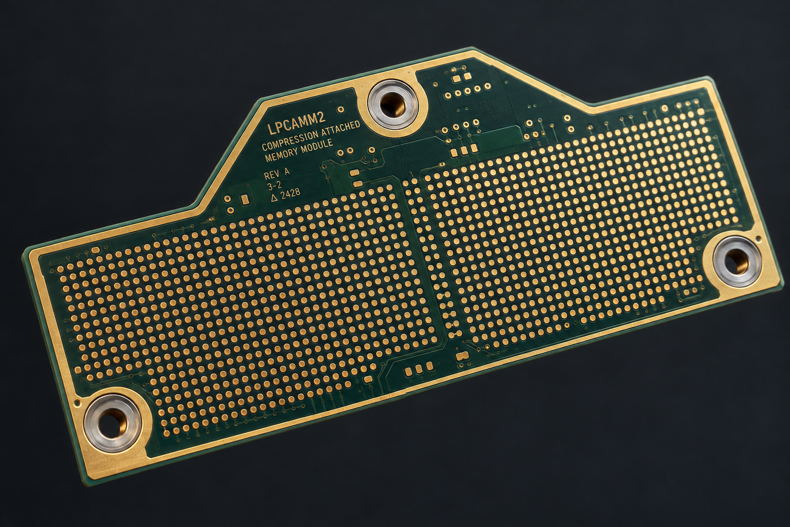
Under the JESD318 specification, the low-power mobile variant is officially designated as LPCAMM2. The engineering elegance of LPCAMM2 lies in its mechanical simplicity and spatial economy:
- The Interposer: Mounted flat against the surface of the laptop motherboard is an ultra-low-profile compression connector or elastomeric interposer measuring less than one millimeter in height. The interposer houses 646 precision-engineered contact springs arranged in a high-density rectangular grid.
- The Module Substrate: The LPCAMM2 module itself consists of a multi-layer printed circuit board measuring just seventy-eight millimeters wide by twenty-three millimeters deep across its main rectangular body, with a trapezoidal handling extension. On its bottom surface, the board features 646 matching gold-plated land pads.
- The Captive Mounting Screws: Instead of spring clips that bend and fatigue over time, the module is secured into place by three captive M2 precision Torx or Phillips screws that thread into metal standoffs anchored through the motherboard.
- Uniform Compression Force: As the three screws are tightened to a specified torque, the module presses evenly downward against the interposer springs. This vertical compression establishes 646 microscopic, gas-tight electrical junctions simultaneously.
Because the contact pads sit directly beneath the memory module rather than along an edge, the physical distance between the processor's memory controller and the DRAM chips is compressed to the absolute minimum. Signal traces route vertically downward from the silicon die, pass through the interposer contacts, and enter the motherboard layers in a direct vertical path of less than 1.5 millimeters. Total trace lengths on the motherboard are reduced from the sixty to eighty millimeters typical of SO-DIMM slots down to twelve to fifteen millimeters.
This radical reduction in physical distance eliminates the parasitic capacitance and signal reflections that previously doomed socketed memory. By preserving a continuous, matched forty-ohm impedance across the entire transmission path, LPCAMM2 enables LPDDR5X memory to achieve data transfer speeds of 7,500, 8,533, and eventually 9,600 megatransfers per second, matching the performance of permanently soldered memory down to the last picosecond while remaining entirely modular.
⚡ Dual-Channel 128-Bit Memory on a Single Compact Card
Beyond solving the signal integrity dilemma, the JEDEC LPCAMM2 standard delivers a masterclass in spatial efficiency by solving an architectural flaw that plagued SO-DIMM systems for a quarter of a century: the multi-socket requirement for dual-channel memory.
To understand why this matters, one must examine how memory buses interface with modern processors. A single channel of standard DDR4 or DDR5 memory provides a 64-bit wide data bus (or two 32-bit subchannels in DDR5). To unlock the processor's full memory bandwidth and feed its integrated graphics execution units, a system must operate in dual-channel mode, establishing a combined 128-bit wide data highway. In the era of SO-DIMM, achieving a 128-bit dual-channel memory bus required installing two physically independent memory modules into two separate sockets.
This requirement created severe architectural penalties for laptop designers. Motherboard engineers had to carve out space for two massive plastic sockets. If the sockets were placed side-by-side, they consumed vast horizontal surface area that pushed the battery and cooling heat pipes out of the chassis. If the sockets were stacked vertically on top of each other, they created a thick physical tower that dictated a chunky chassis profile. Worse, if a cost-conscious consumer purchased a budget laptop configured with only one SO-DIMM stick, the system operated in single-channel mode, cutting memory bandwidth in half and crippling the performance of the integrated GPU.
SO-DIMM Dual-Channel Layout (Inefficient & Bulky):
[Motherboard Surface]
  +====================================================+
  | Slot 1: Channel A (64-bit Bus)                     | ===> Consumes ~1,800 mm²
  +====================================================+      Z-Height: 8.5 to 11.2 mm
  +====================================================+
  | Slot 2: Channel B (64-bit Bus)                     |
  +====================================================+

LPCAMM2 Unified Layout (Ultra-Compact & Complete):
[Motherboard Surface]
  +====================================================+
  | LPCAMM2 Single Module:                             | ===> Consumes ~650 mm² (-64%)
  | Channel A (64-bit) + Channel B (64-bit) = 128-bit  |      Z-Height: 4.5 mm (-58%)
  +====================================================+
LPCAMM2 completely eliminates this constraint. Under the JESD318 specification, a single LPCAMM2 module delivers a complete 128-bit wide memory interface directly out of the box. By routing eight independent 16-bit subchannels from four dual-channel LPDDR5X DRAM dies mounted on the module substrate, a single card provides the processor with its full dual-channel memory bus over its 646 compression contact pads.
The physical implications of this consolidation are clear:
- 64 Percent Surface Area Reduction: A single LPCAMM2 module occupies approximately 650 square millimeters of motherboard area, compared to more than 1,800 square millimeters required for two horizontal SO-DIMM slots. This frees over 1,150 square millimeters for larger batteries, expanded cooling radiators, or secondary M.2 NVMe storage.
- 58 Percent Thinner Profile: When installed, the total vertical height of an LPCAMM2 module is approximately 4.5 millimeters above the motherboard, compared to 8.5 to 11.2 millimeters for stacked SO-DIMMs. This allows integration into chassis well under fourteen millimeters thick.
- Guaranteed Dual-Channel Performance: Every laptop equipped with an LPCAMM2 module operates in full 128-bit dual-channel mode regardless of capacity, eliminating the single-channel performance penalty that historically penalized entry-level configurations.
- Up to 61 Percent Active Power Savings: Utilizing mobile LPDDR5X silicon operating at 0.5 to 1.05 volts rather than DDR5 at 1.1 volts cuts active power by up to sixty-one percent. In standby, deep-power-down modes reduce energy consumption by up to seventy percent compared to DDR5 SO-DIMMs, directly extending battery runtimes.
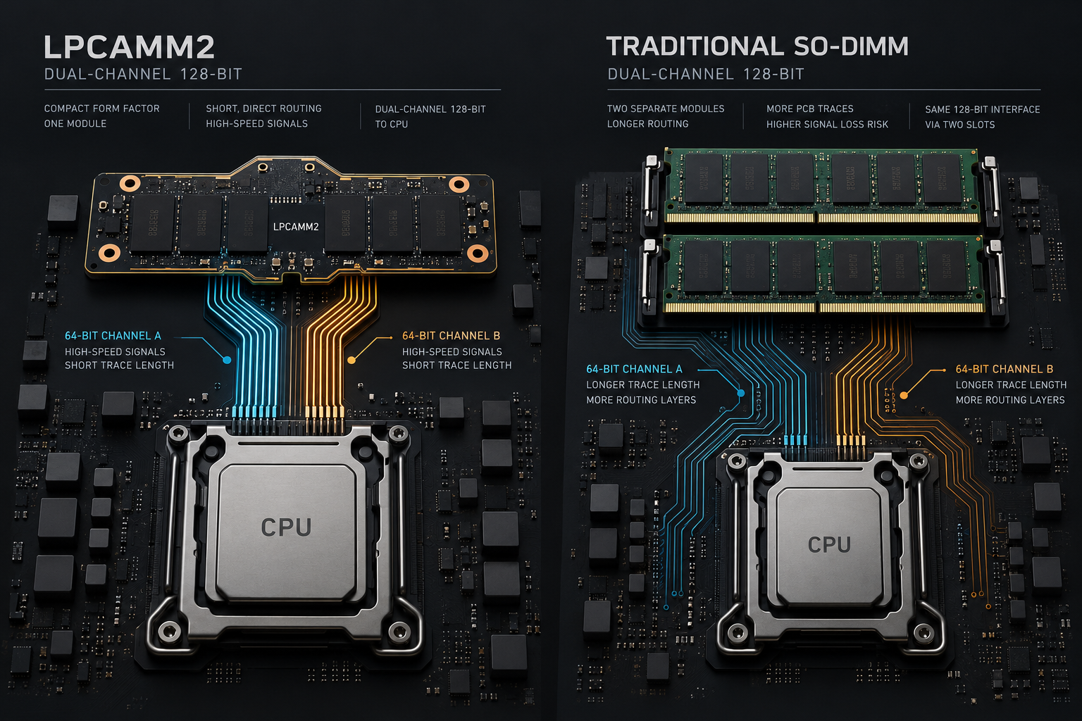
By consolidating dual-channel bandwidth into a single physical card that is thinner, smaller, and vastly more energy-efficient than the legacy sockets it replaces, LPCAMM2 invalidates the industrial design arguments that computer manufacturers previously used to justify soldering RAM to the motherboard.
🔍 The Physical Reality: CAMM2 Versus LPCAMM2 Side by Side
As the JEDEC specification transitioned from committee whitepapers to commercial silicon, it is critical to distinguish between the two distinct mechanical and electrical branches established by the JESD318 standard: standard CAMM2 and mobile LPCAMM2. While both standards share the fundamental Land Grid Array compression philosophy, they are targeted at fundamentally different computing segments and are physically keyed to prevent accidental mismatch.
Standard CAMM2 is engineered for high-performance desktop motherboards, thick gaming laptops, and mobile workstations that utilize standard DDR5 SDRAM. These modules operate at standard DDR5 voltages (1.1 volts) and are designed to replace full-sized desktop DIMM slots or high-power SO-DIMMs. Desktop motherboards adopting CAMM2, such as early demonstrations showcased by Asus, MSI, and Gigabyte, mount the memory module flat against the motherboard surface adjacent to the CPU socket, drastically cleaning up the airflow path around the processor cooler and eliminating the vertical clearance conflicts frequently caused by tall desktop memory sticks.
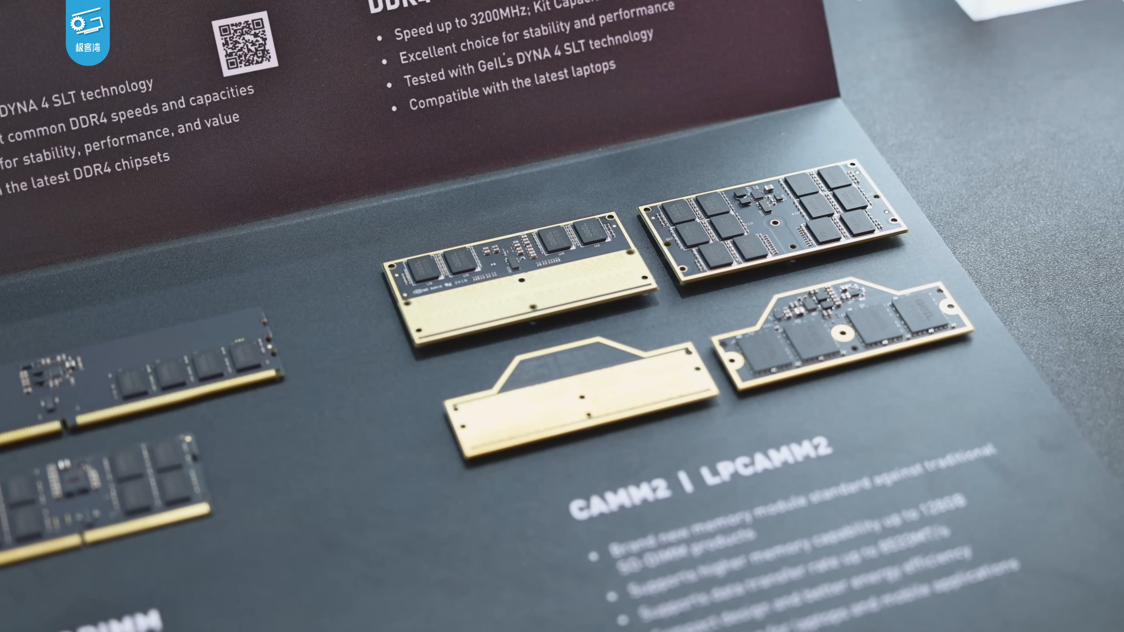
In contrast, LPCAMM2 is the low-power mobile standard designed specifically for ultra-thin laptops, edge AI computing devices, and energy-conscious professional workstations. LPCAMM2 utilizes low-power LPDDR5 or LPDDR5X DRAM silicon. Because standard DDR5 and mobile LPDDR5X utilize entirely different pinouts, signaling voltages, and internal bus structures, JEDEC implemented intentional physical keying differences between the two formats:
- DRAM Technology: Standard CAMM2 uses DDR5 SDRAM; LPCAMM2 uses low-power LPDDR5 or LPDDR5X.
- Operating Voltages: Standard CAMM2 operates at 1.1 volts nominal; LPCAMM2 operates on dual-rail 0.5 volt I/O and 1.05 volt core logic.
- Bus Width: Both provide a 128-bit dual-channel interface, but LPCAMM2 divides this into eight 16-bit subchannels tailored for low-power memory controllers.
- Initial Transfer Speeds: Standard CAMM2 launches between 4,800 and 6,400 MT/s; LPCAMM2 launches between 6,400 and 8,533 MT/s, with clear headroom toward 9,600 MT/s.
- Footprint and Clearance: Standard CAMM2 requires approximately 1,000 square millimeters and includes power management circuitry on the module; LPCAMM2 shrinks to roughly 650 square millimeters with a uniform 4.5 millimeter total height.
- Power Consumption: LPCAMM2 delivers up to 61 percent active power savings and 70 percent standby power savings compared to standard DDR5 implementations.
When viewed side by side, as demonstrated on exhibition floors from Computex Taipei to IFA Berlin, the visual contrast between CAMM2 and LPCAMM2 is striking. Standard CAMM2 exhibits a slightly broader rectangular PCB footprint to accommodate the power management integrated circuits (PMIC) and thermal distribution required by standard DDR5. LPCAMM2, by contrast, is remarkably sleek and compact. Its dark green or matte black circuit board is dominated by four high-density DRAM packages flanking a central routing spine, with its three perimeter screw cutouts reinforcing its utilitarian, service-friendly nature.
Crucially, the JEDEC committee designed the mechanical mounting holes and interposer alignments so that an LPCAMM2 module cannot be physically seated into a standard DDR5 CAMM2 socket, and vice versa. This mechanical lockout protects consumers from catastrophic voltage mismatches while establishing a stable, predictable hardware foundation that third-party memory manufacturers like Micron, Crucial, Kingston, and ADATA can manufacture with universal compatibility.
⚖️ Breaking the Manufacturer RAM Tax and Artificial Margins
While the electrical and spatial accomplishments of LPCAMM2 represent a triumph of microelectronics engineering, the most profound impact of this standard is economic and environmental. By dismantling the technical rationale for soldered memory, LPCAMM2 strikes directly at one of the most lucrative and anti-consumer business models in the modern technology sector: the manufacturer RAM tax.
For over a decade, major computer manufacturers exploited soldered memory as a captive monetization engine. When configuring a laptop on an online storefront, the pricing for memory upgrades bears no relationship to the spot market price of silicon. In recent years, sixteen gigabytes of LPDDR5X silicon cost computer manufacturers between twenty-five and thirty-five dollars at wholesale contract pricing. Yet when a customer clicked the option to upgrade an ultraportable laptop from sixteen gigabytes to thirty-two gigabytes, manufacturers routinely added two hundred dollars to the final bill. Upgrading from sixteen gigabytes to sixty-four gigabytes frequently carried an exorbitant penalty of four hundred to six hundred dollars.
Because the memory was soldered directly to the motherboard, consumers had no alternative. They could not purchase the base model and install affordable third-party memory modules at home, as generations of PC users had done since the 1980s. They were forced to pay the manufacturer's monopoly margin at checkout, or risk owning a computer that would become unusable when their future software demands expanded.
🌍 Reversing the E-Waste Tide with True Repairability
The environmental toll of this business model has been severe. According to data compiled by the United Nations Global E-waste Monitor, the world generated over sixty-two million metric tons of electronic waste in 2022, a figure projected to surge past eighty million metric tons by 2030. Laptops represent a particularly toxic slice of this waste stream because their manufacturing footprint accounts for the vast majority of their total lifetime carbon emissions. Fabricating a modern laptop logic board, etching its multi-layer copper planes, and producing its nanometer-scale silicon chips consumes hundreds of kilowatt-hours of electrical energy and thousands of liters of purified water.
When a laptop features soldered RAM, the entire machine becomes a brittle, single-point-of-failure system:
- Unrepairable Hardware Failures: If a single solder ball beneath one DRAM chip fractures due to thermal cycling, or if an electrostatic discharge damages an internal memory cell, the entire computer fails to boot. Because desoldering and reballing BGA memory packages requires specialized surface-mount rework stations and hours of skilled microscopic labor costing more than the residual value of the machine, authorized service centers refuse to repair the board. Their only protocol is to swap out the entire logic board, consigning pounds of operational silicon, controllers, and circuit traces to the scrap heap.
- Workload Inelasticity: As operating systems and productivity applications integrate local artificial intelligence models, large language models, and complex creative workflows, their baseline memory consumption is escalating rapidly. An eight-gigabyte or sixteen-gigabyte laptop that was perfectly adequate for web browsing and office productivity in 2022 quickly chokes on modern software stacks. With soldered RAM, that laptop cannot be upgraded to thirty-two gigabytes to handle edge AI inference. The owner is forced to discard an otherwise flawless machine with an intact OLED display, functioning keyboard, and healthy battery simply because its memory capacity hit an immovable wall.
LPCAMM2 shatters this premature obsolescence loop. When memory is modular, a catastrophic DRAM failure is resolved in ninety seconds by loosening three screws, swapping in a replacement module, and retightening the fasteners. When a user's computational requirements grow, they can purchase an aftermarket thirty-two or sixty-four gigabyte LPCAMM2 module at open market prices and upgrade their device at their kitchen table. Corporate IT departments can purchase standardized laptop chassis for their workforce and configure memory dynamically based on individual employee needs, extending the operational lifecycle of their enterprise fleet from three years to six or seven years. By separating the lifespan of the memory from the lifespan of the motherboard, LPCAMM2 returns personal computing to the foundational principles of the circular economy.
🚀 From ThinkPad to Framework: The Road to Ubiquitous Modular Computing
The transition from theoretical standard to mass-market reality is already underway. Rather than languishing in prototype limbo, LPCAMM2 has secured high-profile adoptions across the computing landscape throughout 2024, 2025, and 2026.
The watershed moment arrived in April 2024, when Lenovo unveiled the ThinkPad P1 Gen 7, officially becoming the first major PC manufacturer to ship a commercial laptop equipped with LPCAMM2 memory. Engineered with Micron Technology, the ThinkPad P1 Gen 7 proved that a high-end mobile workstation could deliver extreme computational performance with Intel Core Ultra processors and Nvidia RTX graphics while shrinking its chassis profile and retaining fully modular, user-serviceable memory. Lenovo reported that LPCAMM2 saved sixty-four percent of motherboard space compared to standard SO-DIMMs while consuming up to sixty-one percent less active power.
Lenovo expanded this commitment with subsequent workstation generations, including the ThinkPad P1 Gen 8 and Gen 9, which incorporated Micron's 1-gamma DRAM fabrication node to push LPCAMM2 memory capacities up to sixty-four and 128 gigabytes at 7,500 and 8,533 megatransfers per second. Lenovo also introduced LPCAMM2 options into its mainstream commercial enterprise fleet, including the ThinkPad T-series, signaling that modular compression memory was a viable architecture for everyday business laptops.
Simultaneously, the modular computing revolution received a boost from the open hardware community. Framework Computer, the vanguard of the modern right-to-repair movement, officially embraced LPCAMM2 for its ultra-portable laptop lines, culminating in the Framework Laptop 13 Pro. By pairing Intel Core Ultra Series 3 processors with modular LPCAMM2 memory modules delivering 7,467 megatransfers per second, Framework demonstrated that an ultra-portable thirteen-inch laptop could achieve twenty hours of real-world battery life, razor-thin aesthetics, and class-leading repairability without sacrificing a single megatransfer of memory bandwidth.
Looking ahead, the momentum behind compression-attached memory appears unstoppable. The semiconductor industry has already confirmed that upcoming DDR6 and LPDDR6 memory specifications, operating at speeds exceeding 12,000 megatransfers per second, will physically mandate compression-attached form factors like LPCAMM2 for modular implementations. The electrical physics of multi-gigahertz digital signaling have simply outrun the physical limits of pin-and-socket connectors forever.
For fifteen years, the personal computer industry asked consumers to accept an artificial trade-off: surrender your right to repair, pay inflated memory prices, and accept premature electronic obsolescence in exchange for a thin, elegant laptop that lasts all day on battery. With three standard screws, an array of 646 microscopic compression pads, and an open standard ratified by the entire microelectronics industry, LPCAMM2 has definitively proven that the trade-off was a lie. The era of the soldered laptop motherboard is officially drawing to a close, and portable computing is finally returning to the hands of the people who buy it.
Data and technical sources: JEDEC Solid State Technology Association Standard JESD318 CAMM2 Common Specification; JEDEC Annex JESD318-F0-RCE; Micron Technology Memory Architecture Whitepapers; Framework Computer Engineering Technical Specifications; iFixit Hardware Teardown and Serviceability Analysis; Dell Technologies Client Solutions Engineering Documentation.